

CS61C | lecture10
NAND

| a | b | c |
|---|---|---|
| 0 | 0 | 1 |
| 0 | 1 | 1 |
| 1 | 0 | 1 |
| 1 | 1 | 0 |
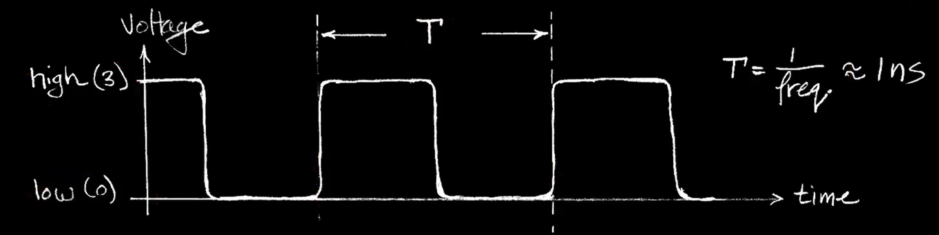
Signals and Waveforms
Clock
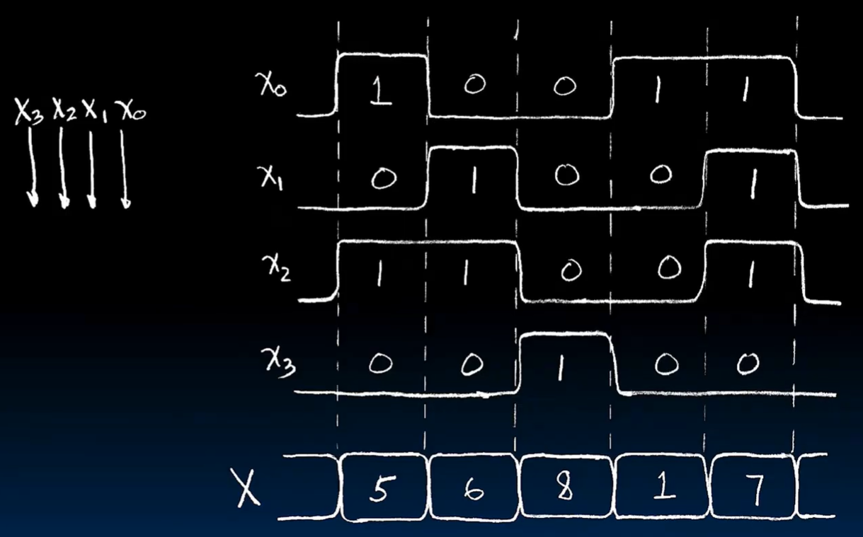
Grouping
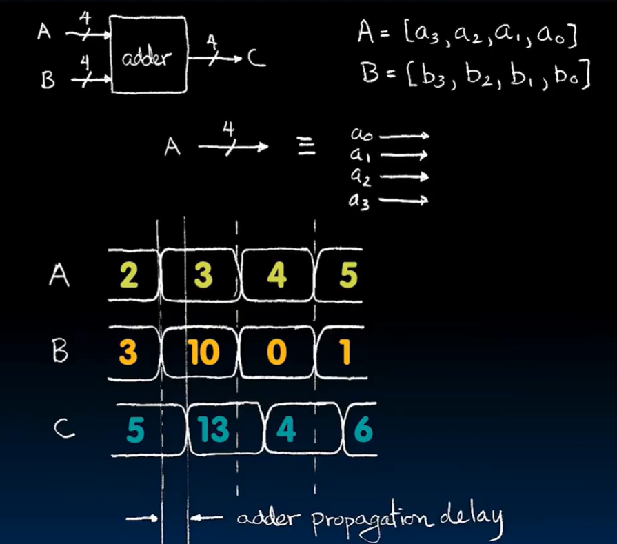
Circuit Delay
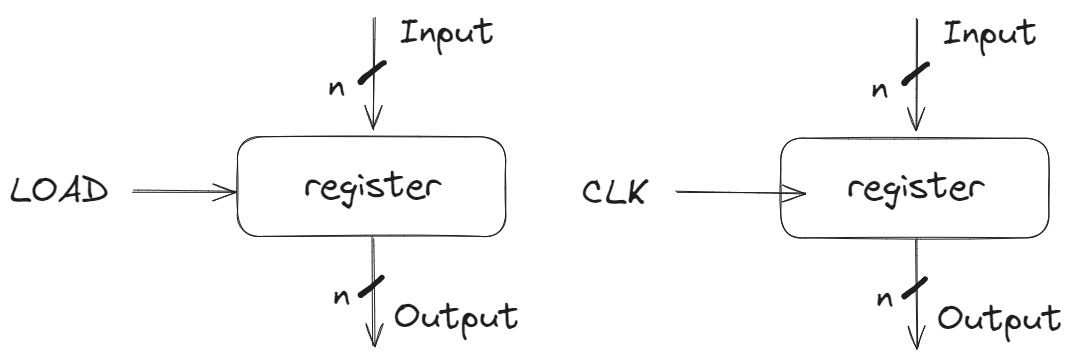
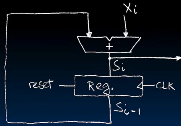
Circuits with State(e.g. register)
Accumulator
1 | S = 0; |
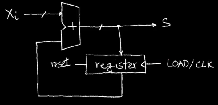
Register is used to hold up the transfer of data to adder.
When reset line is asserted or goes one, the register will be reset.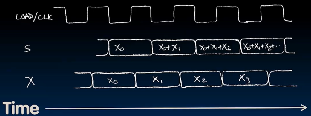
Register Details Flip-flops
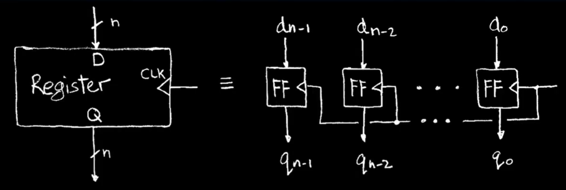
一个 n 位寄存器实际上是 n 个 1 位触发器。
D input is Data, Q is output
这些也叫做 D-type Flip-Flop
上升沿触发(rising edge-triggered)
当它从 0 变为 1 时,就会触发。
On the rising edge of the clock, the input d is sampled and transferred to the output. At all other times, the input d is ignored.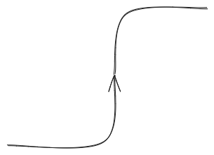
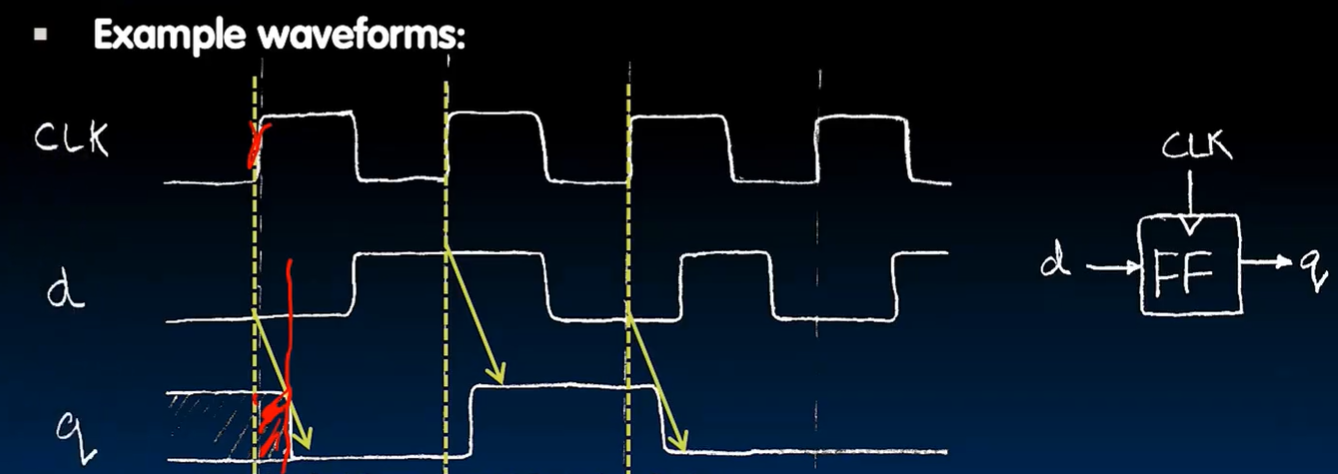
q 中刚开始的阴影部分代表可能是 1 也可能是 0。红色部分是因为存在一定延迟。
Example(more detail)
Accumulator Revisited

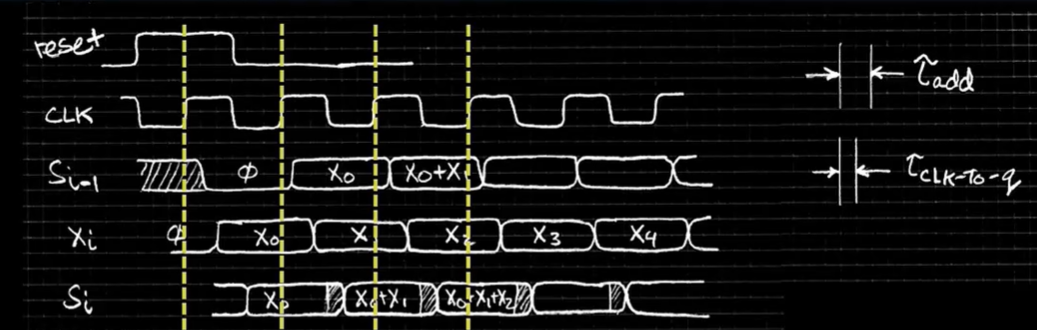
- Reset signal shown.
- Also, in practice X might not arrive to the adder at the same time as $S_{i-1}$
- $S_i$ temporarily is wrong(底下阴影部分), but register always captures correct value.
- In good circuits, instability never happens around rising edge of clk.
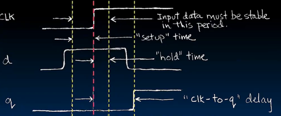
| Clock(CLK) | steady square wave that synchronizes system |
| Setup Time | when the input must be stable before the rising edge of the CLK |
| Hold Time | when the input must be stable after the rising edge of the CLK |
| CLK-to-Q | Delay — how long it takes the output to change, measured from the rising edge of the CLK |
| Flip-flop | ont bit of state that samples every rising edge of the CLK |
| Register | several bits of state that samples on rising edge of CLK or on LOAD |
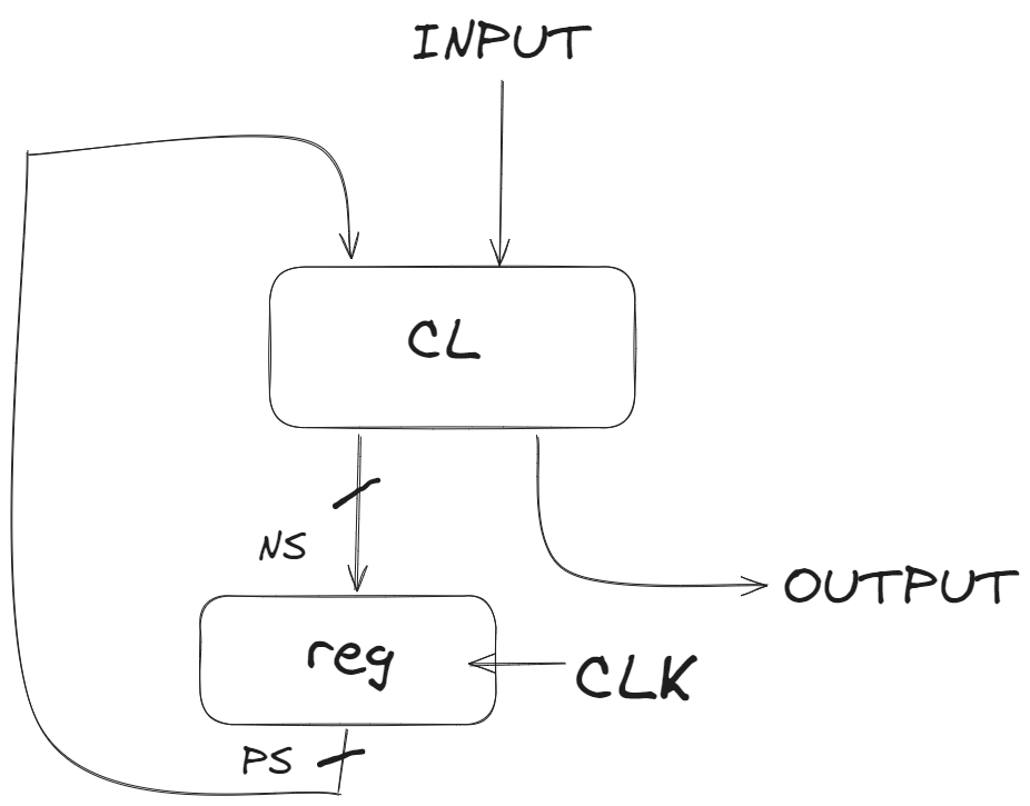
Finite State Machines(FSM) 有限状态机
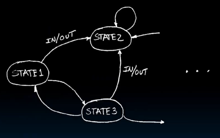
Example: 3 ones
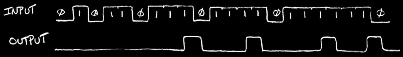
流程如图:
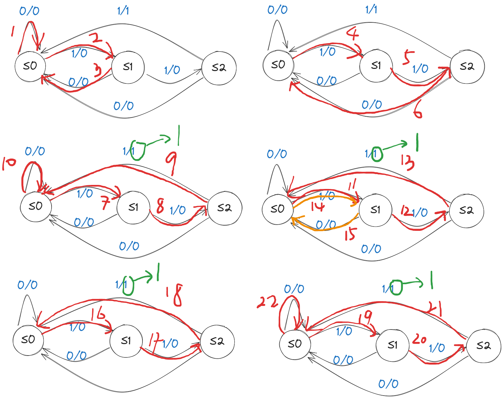
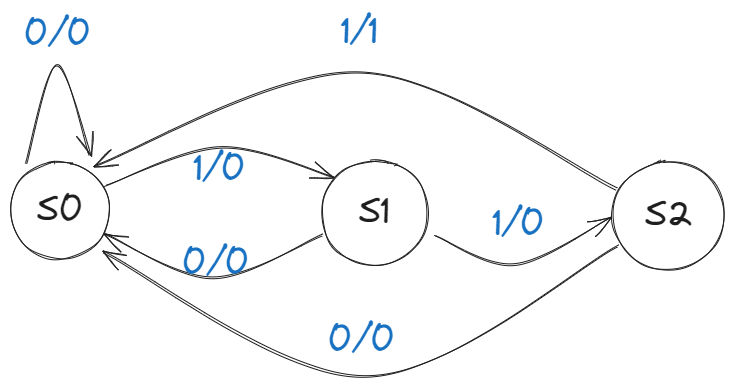
Hardware Implementation of FSM
| PS | Input | NS | Output |
|---|---|---|---|
| 00 | 0 | 00 | 0 |
| 00 | 1 | 01 | 0 |
| 01 | 0 | 00 | 0 |
| 01 | 1 | 10 | 0 |
| 10 | 0 | 00 | 0 |
| 10 | 1 | 00 | 1 |
本博客所有文章除特别声明外,均采用 CC BY-NC-SA 4.0 许可协议。转载请注明来自 Birdy の 小窝!
 wechat
 alipay
相关推荐


评论